- Home
- About Us
- Products
- News & Events
- Service
- Contact Us
Bonders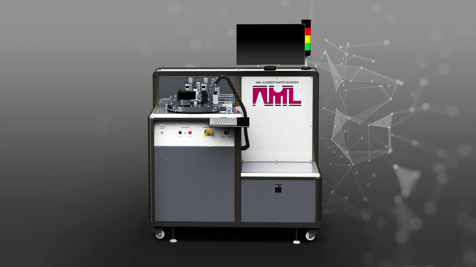 AML - AWB 04 & 08 Platform
The AWB has the versatility to perform aligned: Alignment & bonding in one machine
Automatic PC Control & Data acquisitionLive control of all bond parameters or fully automated recipes. All the bonding parameters e.g. current, voltage, integrated charge, temperature, chamber pressure, force, wafer separation, run parameters, recipes, wafer batch No for SPC and event logs are automatically stored in files for graph plotting and trend analysis. Machines can also be networked and remotely interrogated by AML to aid fault finding. Fully automatic recipe, including auto alignment to deskill operation in a production environment. Alignment:Manual and auto alignment. In-situ alignment has advantages over other bonders (where alignment is made outside the bond chamber).‘One click’ align and bond. Visible and IR. Image capture for widely spaced 3D alignment marks. Alignment can be carried out hot or cold:This eliminates alignment inaccuracies due to thermal expansion & mismatch between wafers, machine parts & platens. Large wafer separation:Allows large temperature difference between wafers – ideal for better activation or in-situ oxide reduction via process gas e.g. forming gas. Also allows fast, high vacuum & well defined bonding environment. In-situ system:Also enables visual confirmation just before the bonding process that the desired alignment is still being achieved. Wafer sizes:2”, 3", 4", 5”, 6” & 8”. (Also chips & odd shaped substrates, but without alignment). Manipulator:
Enables in-situ alignment of wafers under vacuum and at elevated temperature. Optics:Twin Microscope – camera system with throughthe-lens illumination. Two CCD cameras and side-by-side display of images. Including IR capability. Simultaneous display of wafer separation & bonding force for complete alignment control. BondingEnvironment:Vacuum, or process gas. Fully automated dry turbo pumping system ~ 1x10⁻⁶ mbar to 2bar absolute pressure. UHV option Temperature:Both Upper & Lower Platens independently adjustable in 1 °C steps. Heating & Cooling rates are programmable. Max Temperature is 560°C. Electrodes:(for Anodic Bonding)
Full size heated platens for both upper andlower electrodes for better bond uniformity. 0-2.5 kV DC up to 40 mA. Constant current or voltage operation, for improved process control & stress management. Additional Options:
|
|
